


What to Buy in Semi Downcycle? – An Introduction to TSMC N2 & A16/A14 Beneficiary Plays

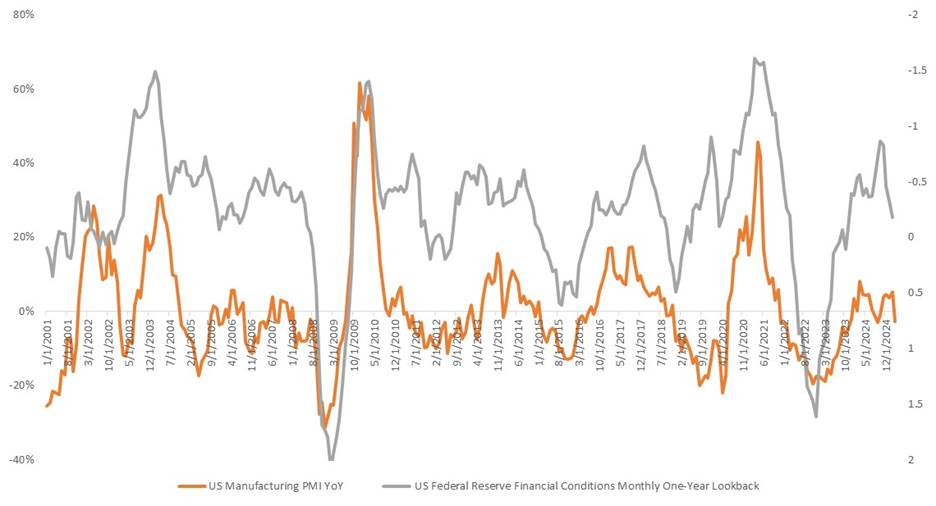
I introduced in my last year’s article (Has SOX peaked out? – A personal view on the current semiconductor cycle) that the most related indicator to the semiconductor cycle is the US Manufacturing PMI YoY Growth. Historically, whenever the YoY growth rate of the US Manufacturing PMI drops to around 0% level, it triggers a sharp decline in the SOX (Philadelphia Semiconductor Index), marking the end of a semiconductor cycle. In addition, the leading indicator of the US Manufacturing PMI YoY is US financial conditions. At present, both of these two indicators appear unfavorable, indicating that we have entered a semiconductor downcycle (see chart below):
In today’s article, we will discuss: What stocks should one buy if they want to bottom-fish during a semiconductor downcycle? In fact, I was initially a contrarian investor, enthusiastic about buying stocks on the left side of the cycle. But after more than ten years of experience in the capital market and suffering many times of losses, I have summarized three stock-picking principles for bottom-fishing during a downcycle:
1. The company’s own balance sheet does not have excessive debt and can support the company through the industry downcycle (i.e., ensure the stock won’t blow up);
2. The company has high certainty that its business can resume growth in the foreseeable future (i.e., buy high-probability stocks, so one can confidently continue to add positions during price drops);
3. The company’s business can meaningfully outperform the industry’s average growth rate in the next upcycle (i.e., buy stocks that can outperform the market).
In today’s semiconductor industry, there is one investment theme that meets the above bottom-fishing criteria: that is the beneficiaries of TSMC’s N2 and A16/A14 processes. We know that TSMC will switch from FinFET to GAA architecture in its N2 process, and will further adopt backside power delivery network in its next-generation A16/A14 process. Such a structural transformation will undoubtedly benefit a group of semiconductor equipment and materials suppliers, enabling them to enjoy growth rates exceeding the industry average in the next semiconductor upcycle. Moreover, TSMC’s investment in N2 and A16/A14 processes is almost ~100% certain, with Fab20, Fab21, Fab22, and Fab25 all having expansion plans for N2 and A16/A14.
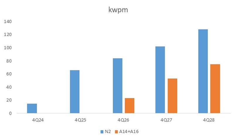
The table below lists TSMC’s capacity planning for N2/A16/A14 over the next 4 years. We can see that its N2 process is planned to expand from 15kwpm in 4Q24 to 128kwpm in 4Q28 (equipment basis, including the new US fabs), and its A16/A14 process is planned to expand from 23kwpm in 4Q26 to 75kwpm in 4Q28 (equipment basis, including the new Taichung fab):
Next, I will briefly introduce the transition from FinFET to GAA in TSMC’s migration from N3 to N2 process, and the transition to backside power delivery network in the migration from N2 to the next-generation A16/A14 process.
As shown in the figure below, the structure of semiconductor transistor was originally a 2D planar structure, where the gate controlled whether current (on or off) flows from the source through the channel to the drain:

However, as the width of the channel continues to shrink, once it shrinks to a certain point, leakage begins to occur: That is, when the gate attempts to shut off the current, due to the channel wall being too thin, the current directly breaks through the wall and still flows from the source to the drain, and the gate can no longer completely control the current. This is reflected at the chip level as significantly higher power consumption in the produced chip.
In order to solve the leakage issue, process nodes below 22/20nm began to adopt 3D structure (see figure below). From 14nm to the latest 3nm process, all adopt the FinFET (fin field-effect transistor) structure: The channel protrudes and is surrounded on three sides by the gate, greatly enhancing the gate’s control over the channel. It is named FinFET because the protrusion resembles a fish fin (the left diagram is a 3D view, and the right diagram is a cross-sectional view):

However, the FinFET structure began to encounter leakage issues again below 10nm. Therefore, starting from the 2nm process, TSMC will adopt a brand-new 3D structure—GAA. In this structure, each channel is completely surrounded by the gate on all four sides, further enhancing the gate’s control over the channel and preventing leakage. GAA (gate all around) is named for this reason (the left diagram is a 3D view, and the right diagram is a cross-sectional view):

Furthermore, TSMC’s next-generation A16/A14 processes (i.e., 1.6nm/1.4nm) introduce a backside power delivery network (BPDN) on top of the GAA architecture. The BPDN technology moves the power rails outside of the logic elements, thereby reducing the size of logic device. Compared to front-side power delivery, backside power delivery has better energy efficiency, more complete signal transmission, lower voltage drop, better wire space design, and lower producing cost, making it more suitable for AI chip applications:

BPDN requires only 4 metal layers to connect the power lines through micro vias to the contact layer (i.e., the transistor layer), while front-side power delivery requires as many as14 layers (see figure below). In front-side power delivery, the width of copper wires becomes smaller and smaller with each lower layer, and the manufacturing cost correspondingly increases. BPDN can greatly shorten the path between the bump and the transistor, thereby reducing voltage drop issues. When producing advanced node chips, especially those AI chips with large-scale wiring structures, the advantages of backside power delivery become increasingly important.

Currently, BPDN technology is divided into three architectures: Buried Power Rail, Power Via, and Direct Backside Contact to Source/ Drain:
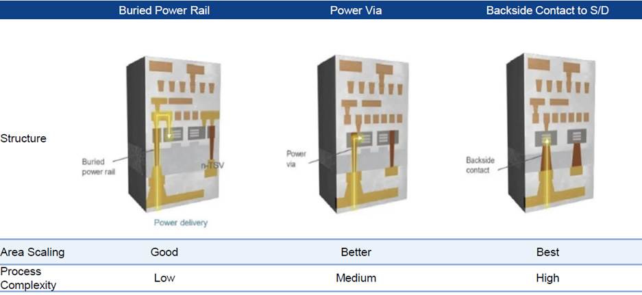
Buried Power Rail is the simplest way to implement backside power delivery. Essentially, it connects the via on the backside power rail upward to the area around the CMOS FET, and then downward to the top contact. This power rail method was originally developed by IMEC in 2019, but no company in the industry has really used it for mass production.
The second method, Power Via, is slightly more complex. It allows the via to extend from the front side to the front contact, offering a greater scaling advantage than Buried Power Rail. Intel is the first player to introduce Power Via technology in its Intel 18A process in 2025. Samsung plans to adopt BPDN in its SF2Z process in 2027, using a technology similar to Power Via with µTSV to connect the transistor.
The third method, Direct Backside Contact to Source/ Drain, is the most challenging to implement, but it also brings the best chip performance and size scaling advantages. In this solution, the backside via directly contacts the source or drain of the transistor from below. This means the wafer needs to be thinned and etched until almost no silicon substrate remains (~10nm thick). In addition, the lithography patterns on both sides of the BPDN wafer must be perfectly aligned, requiring extremely high precision in system control and equipment. TSMC plans to introduce Super Power Rail technology, a BPDN technology with Direct Backside Contact to S/D, starting from the A16/A14 process in 4Q26.
In the following paragraphs, I will introduce four semiconductor equipment and materials companies that truly benefit from TSMC’s N2 and A16/A14 process transitions, and two “fake” beneficiaries mistakenly perceived by the market.
Keep reading with a 7-day free trial
Subscribe to Global Technology Research to keep reading this post and get 7 days of free access to the full post archives.