


NVIDIA (NVDA US) GB300, Vera Rubin & Beyond – An Update on Future PCB/CCL and Power Design Change

In the last year’s article, I introduced the PCB design (Is Amphenol Overpass Replaced by PCB? – All you need to know about GB200 NVSwitch tray redesign issue) and power system design (Is Monolithic Power System (MPWR US) a Short? – The GB200 Power Module War) of NVIDIA’s GB200. Today, I will continue to explain changes in PCB, CCL, and power design in its latest GB300 and subsequent VR200, as well as future R&D projects.
First of all, let’s review the compute tray design of GB200: Each compute tray consists of two Bianca boards. Each Bianca board is essentially a 22-layer HDI board, of which 18 layers (build-up layers) use M8 materials and 4 layers (core layers) use M4 materials. These are mainly supplied by Unimicron in Taiwan and Victory Giant Technology in mainland China.
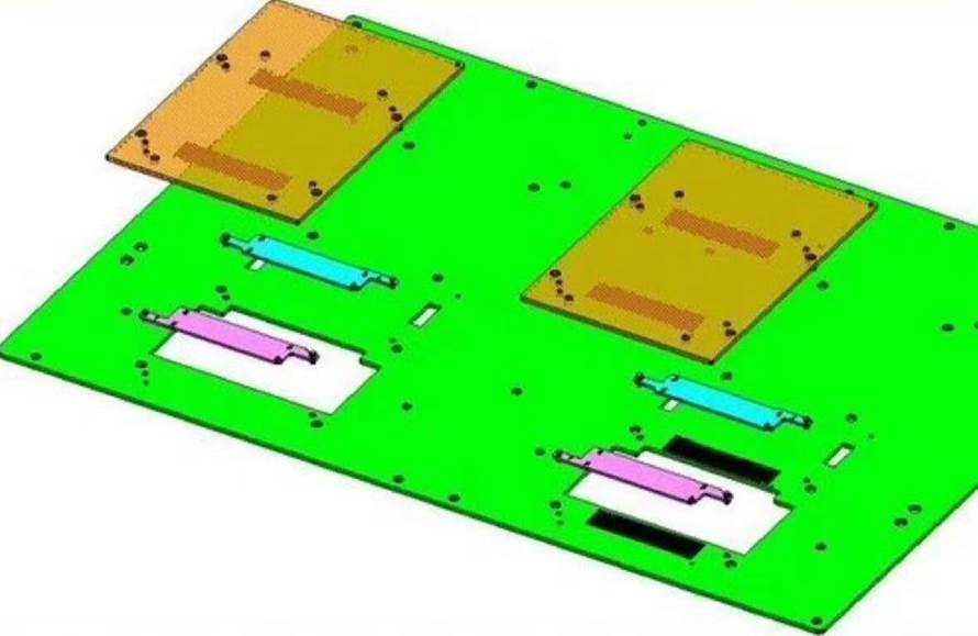
For GB300, NVIDIA adopted a completely different design from GB200 in order to avoid accusations from the U.S. government of using its GPGPU monopoly for bundle sales, as well as to improve production yields for downstream ODM manufacturers. Each GB300 compute tray has only one large PCB, reverting to the UBB (Universal Base Board) + OAM (OCP Accelerator Module) design from earlier HGX products. The Grace CPU in GB300 is still directly SMT-mounted onto the UBB, while the Blackwell GPU gets connected to the OAM via a GPU socket. The GPU signals are then routed through the OAM’s copper wires to the underlying UBB (see the diagram below: green for UBB, yellow for OAM, and blue/ purple for sockets). This design allows downstream ODMs to remove the expensive Blackwell GPU via the socket when assembly issues occur, saving costs compared to the current GB200 design where the GPU is directly mounted on the Bianca board.
The GB300 UBB is an 18-layer PTH (Plated Through-Hole) board, with 14 layers using M8 materials and 4 layers using M4 materials. A single UBB has an ASP of approximately $750–$800, mainly supplied by WUS in mainland China and TTM in the U.S. The OAM on top of the UBB has two design variants:
The high-end version, with 2 Grace CPUs + 4 Blackwell GPUs, uses a 20-layer PTH board, with 16 layers of M8 material and 4 layers of M4 material, supplied by WUS and TTM.
The low-end version, with 1 Grace CPU + 4 Blackwell GPUs, uses a 16-layer HDI board, with 12 layers of M8 material and 4 layers of M4 material, supplied by Unimicron and Victory Giant Technology.
The ASP for a single OAM is approximately ~$100.
The CCL for the GB300 compute tray is exclusively supplied by Doosan in South Korea. The NVSwitch tray PCB/CCL design remains the same as GB200, using a 22-layer M8U PTH board, with PCBs supplied by WUS and TTM, and CCL exclusively supplied by Elite Material (please refer to my previous article for more details: Is Amphenol Overpass Replaced by PCB? – All you need to know about GB200 NVSwitch tray redesign issue).
In the following paragraphs, I will discuss changes in power design (VRM & PDB) in the GB300 compute tray, and potential technology upgrades in the upcoming Vera Rubin generation (eg. PTFE, HVDC, power racks, etc.).