


NVIDIA (NVDA US) 2025 GTC Review – Is Amphenol (APH US) Dead Beyond NVL72?

I first wrote an article about NVIDIA 2025 GTC Preview back in February this year (NVIDIA (NVDA US) 2025 GTC Preview -- An Update on its Latest CPO Switch and NVL288 Design). Some readers may ask: the GTC conference was held in March, so why write a GTC review only now? The answer is: I’m lazy… (just kidding :)). Actually, I didn’t originally plan to write a review article, but after seeing that many Substack authors have been publishing their own GTC reviews one after another, I figured that I’d follow the trend and write one too.
Since I have started relatively late, most of the content released at NVIDIA’s 2025 GTC has already been thoroughly analyzed. So today I’ll take a different approach and discuss a topic that’s still relatively underexplored by investors: the “content dollar” problem of Amphenol in NVIDIA’s future AI server product roadmap. I first wrote about Amphenol (APH US) in an article published in early September last year (Is Amphenol Overpass Replaced by PCB? – All you need to know about GB200 NVSwitch tray redesign issue), and since then, the market has been concerned about Amphenol’s shrinking content dollar in NVIDIA’s server rack. Apart from the NVSwitch tray in GB200/GB300 systems transitioning from using overpasses to a PCB design, the next-generation concept machine Kyber 3, showcased at this year’s GTC, didn’t feature any overpasses or cable cartridges at all (see image below). This further deepened investor concerns that Amphenol might lose its content share in NVIDIA’s future AI server products:
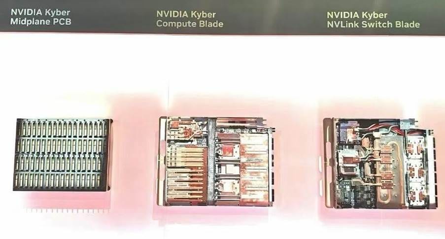
We now know that the Kyber 3 rack contains a total of 4 canisters, each canister housing 18 compute blades at the front, with each blade containing two GB200s, and each GB200 containing two Blackwell GPUs. So the entire rack has 4 x 18 x 2 x 2 = 288 Blackwell GPUs. This is the original concept of NVIDIA’s 288-GPU dense rack (NVIDIA (NVDA US) GB300, Vera Rubin & Beyond – An Update on Future PCB/CCL and Power Design Change). However, based on NVIDIA’s new naming convention, each GPU die is now counted separately. Since each Blackwell GPU includes two GPU dies, the Kyber 3 rack is now referred to as an NVL576 rack (288 x 2 = 576).
However, here’s an issue that some readers may not have noticed: it only shows 72 Blackwell GPUs within a single canister (i.e., the Kyber Compute Blades), which are connected via an orthogonal backplane (i.e., Kyber Midplane PCB) to the NVSwitches (i.e., Kyber NVLink Switch Blades), forming NVL72 interconnect. However, the GTC showcase did not reveal how the four canisters in the entire Kyber rack are interconnected to each other to achieve NVL288/NVL576.
If we take a closer look at the Kyber rack shown at GTC, we can see that there are a total of 8 blades inserted at the back of each canister. 6 of them are NVLink Switch Blades, with each blade containing three switch chips. In addition, there’s one Management Blade on each side, which is unrelated to NVLink and is used independently for system management (see image below: green boxes are NVLink Switch Blades, red boxes are Management Blades):
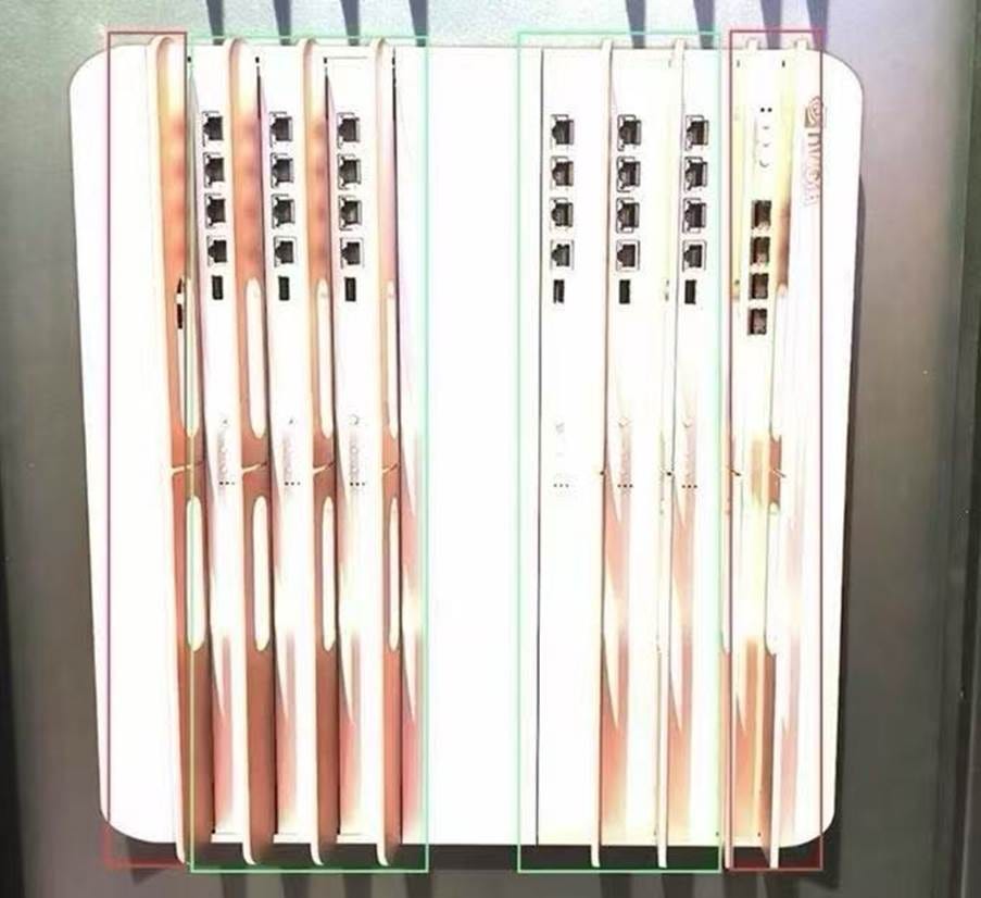
From the image above, it is clear to see that neither the NVLink Switch Blades nor the Management Blades have NVLink uplink interfaces on their rear end — only management interfaces are present. Therefore, the Kyber rack showcased at this year’s GTC is more accurately described as NVL72 x 4 rather than NVL288/NVL576. Its four canisters operate completely independently. The NVSwitch Blades at the back of each canister only provide NVLink downlink interfaces on the front side of the blades, connecting via high-speed connectors to the Midplane PCB and then to the Compute Blades in front, thus completing the NVL72 interconnection. But under the current architecture, each canister (i.e., each group of 72 GPUs) exists independently and is not interconnected with the others via NVLink.
So how does the complete version of the Kyber rack actually achieve NVL288/NVL576 interconnect? Let me explain further in details below:
Keep reading with a 7-day free trial
Subscribe to Global Technology Research to keep reading this post and get 7 days of free access to the full post archives.