Mitsui Mining & Smelting (5706 JP) – An Introduction to SLP, MSAP, and CoWoP Technology
I first introduced the Japanese high-end electronic copper foil manufacturer Mitsui Mining & Smelting (5706 JP) in an article earlier this year. However, that article mainly focused on Mitsui Mining’s HVLP copper foil product (NVIDIA (NVDA US) 2025 GTC Preview -- An Update on its Latest CPO Switch and NVL288 Design). Recently, as investors’ interest in NVIDIA's CoWoP (Chip-on-Wafer-on-Platform PCB) technology has surged, I will introduce Mitsui Mining’s another high-end electronic copper foil product in today’s article: carrier copper foil.
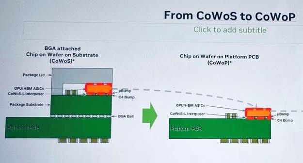
First of all, we know that TSMC’s CoWoS technology is an advanced 2.5D packaging technology. Simply put, CoWoS (Chip-on-Wafer-on-Substrate) integrates multiple chips (such as GPUs and HBMs) onto an interposer, which is then packaged onto a substrate. I have given a detailed explanation of this in an article earlier last year (The Bonder War – An update on ASMPT (522 HK),BESI (BESI NA), Shibaura (6590 JP), Tazmo (6266 JP) and other advanced packaging equipment players). CoWoP is an evolved version of CoWoS technology, replacing the substrate with a PCB. That is, it eliminates the traditional ABF substrate, allowing chips to be directly connected to the platform PCB through RDL wiring on the interposer. This simplifies the packaging structure, resulting in thinner form factor, less signal loss, and better thermal performance (see diagram below):
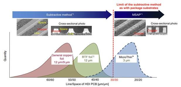
Under the CoWoP process, the platform PCB must directly carry the wafer, which significantly raises the requirements for line/space precision in the bonding area: whereas traditional server PCBs typically have a line/space of around 50 micrometers, CoWoP must achieve below 30 micrometers, even down to 10–15 micrometers. PCBs with line/space below 30 micrometers fall under the category of Substrate-Like PCBs (SLP) and must adopt the MSAP (Modified Semi-Additive Process) technique. The conventional subtractive process is no longer suitable for making such PCBs (see diagram below):
As we know, traditional PCBs use the so-called subtractive process, which involves laying down a full layer of thick copper and then using etching solution to remove unwanted parts to form the desired circuit pattern. However, this method struggles to produce fine lines and is prone to issues like uneven etching and pattern distortion. The MSAP process, by contrast, is a modified semi-additive method. It directly electroplates circuits on a carrier copper foil, and later removes the carrier layer to form ultra-fine circuit patterns, achieving line/space of 10–30 micrometers (see diagram below):
Compared to the subtractive process, the MSAP process has the following two advantages:
1. Finer lines: MSAP supports minimum line/space of 10μm, increasing routing density to meet high-speed/ high-frequency packaging demands.
2. Straighter and more uniform copper lines: MSAP avoids issues such as undercutting and line width inconsistency found in traditional etching process.
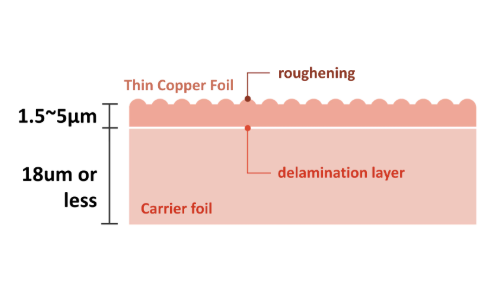
The carrier copper foil used in the MSAP process is a special structured copper foil, typically composed of two bonded copper layers:
· Functional Copper Layer: This is the layer that ultimately forms the circuit pattern. It is extremely thin, usually available in 1.5μm, 3μm, and 5μm thicknesses spec.
· Carrier Layer: This layer provides mechanical support to the functional layer, with a thicker profile (usually 18μm), and is removed during later processing stages (see diagram below):
SLP (Substrate-Like PCB) manufacturers laminate the entire carrier copper foil onto a resin film, and then peel off the supportive carrier layer to proceed with the ultra-thin functional copper layer. The thicker carrier layer provides mechanical rigidity, protecting the ultra-thin functional layer from damage during early manufacturing stages and enabling more precise pattern transfer. Japan’s Mitsui Mining & Smelting (5706 JP) holds a monopoly position in the global carrier/ ultra-thin copper foil market, with nearly 100% market share.
In addition, CoWoP packaging technology also imposes higher performance requirements on the PCB materials used:
· Surface Quality: Traditional CoWoS involves packaging chips before soldering them to the PCB, so surface quality demand is lower. In CoWoP, however, wafers are directly bonded to the SLP, which demands higher flatness, roughness, and cleanliness of the PCB surface in order to avoid cracks or connection failures during bonding process.
· Coefficient of Thermal Expansion (CTE): Similarly, since CoWoP connects wafers directly to the SLP, the materials used must move toward lower CTE value, matching that of the wafer as closely as possible to avoid delamination or cracking issue caused by inconsistent thermal expansion and contraction.. This includes:
o Glass Fiber: Conventional AI server PCBs require low Dk/Df glass cloth. Once bonded directly with chips, it also needs to meet low CTE requirements (i.e., T Glass or V Glass, see bottom right of the diagram below).
o Resin Materials: Traditional epoxy resin is no longer suitable; it must transition to BT (bismaleimide triazine) resin to increase Tg (glass transition temperature) and reduce CTE variation under high temperatures.
In the following paragraphs, I will try to estimate the impact of AI applications on the carrier copper foil market:
Keep reading with a 7-day free trial
Subscribe to Global Technology Research to keep reading this post and get 7 days of free access to the full post archives.


