As a former blue-chip stock in Japan's semiconductor sector, Lasertec (6920 JP) has seen its stock price fluctuate significantly in recent months. A few months ago, a short-seller published a report criticizing the company, leading to a sharp drop in its stock price. Lasertec later released a strong earnings report during its latest earnings call, effectively countering the short-sellers and the hedge funds betting against it. Indeed, Lasertec's last quarter earnings was impressive, especially with its new orders seeing significant growth, surprising many investors.
Nevertheless, during Lasertec's last earnings call, one interesting point caught my attention. When the new president of the company was answering a question from a sell-side analyst, he mentioned that in the company’s mask inspection tool order backlog, the proportion of orders from mask shops and wafer fabs was about 50:50. From a top-down perspective of total addressable market (TAM), the market size for mask inspection tools used in wafer fabs should be much larger than that for mask shops. As Lasertec holds a monopoly position in the EUV mask inspection tool market, shouldn't the proportion of orders from wafer fabs in its order backlog be much higher than from mask shops? Why did the company’s president say the ratio was 50:50?
To answer this question, we need to have a comprehensive understanding of the EUV mask inspection tool market in which Lasertec operates. First, let's revisit a fundamental question: Why does advanced semiconductor processes node require EUV lithography?
We know that a semiconductor lithography tool is an optical imaging device, and its resolution limit (minimum critical dimension) follows the Rayleigh criterion in physics:
In this formula, λ(lambda)is the wavelength of the light source used by the lithography tool, NA (numerical aperture) refers to the amount of light the optical system can collect, and K1 is an optical coefficient. The table below shows three sets of parameters (λ/NA/K1) for lithography systems using different light sources, and the ultimate resolution they can achieve (see CD or resolution row below):
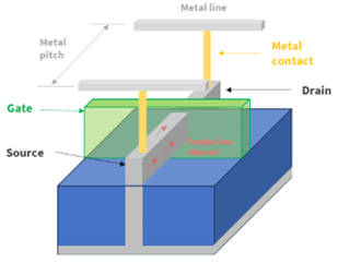
In simple terms, a semiconductor chip is made up of numerous transistors, and a transistor consists of a source, a drain, and a gate. The gate controls whether current flows from the source to the drain (see the diagram below):
In semiconductor manufacturing process, the term “node” originally referred to the distance between two adjacent smallest transistors within a chip. Of course, nowadays, the naming of advanced processes by foundries no longer follows this definition and has become more of a marketing term. The table below shows the minimum transistor pitch for each generation of advanced processes from 7nm node onward (see the "metal pitch" row):
Here, we need to understand one important point: The resolution limit (CD min) of a lithography tool, as determined by the Rayleigh criterion, is approximately equal to half the minimum transistor pitch shown in the table above. This is because the pitch size theoretically measures the center-to-center distance between two adjacent transistors (see the diagram below), while CD refers to the smallest pattern a lithography tool can print, i.e., the gate of the smallest transistor. In the past, when transistors were still in 2D structure, the width of the gate was about half the transistor pitch, so it has become a de facto industry formula that CD min = min metal pitch / 2. Of course, with the shift to 3D transistor structure, the gate width is no longer exactly half the transistor pitch.
By comparing the two tables above, we can see that the minimum CD achievable by an ArF immersion lithography tool is 27.6nm, while the minimum metal pitch for the 7nm process is 40nm. Since 27.6nm > 40nm / 2, the industry began using EUV lithography tool starting from the 7nm process. Moving forward, the next generation of High NA EUV will be needed. The term High NA EUV refers to a lithography tool that still uses a 13.5nm EUV light source, but improves the numerical aperture by enhancing its optical system (e.g., using larger mirrors, increasing the opening of the light cone, etc.), thereby improving the resolution limit (CD min):
Theoretically, the 2nm process should begin using High NA EUV (min metal pitch 22nm / 2 = 11nm = High NA EUV CD), but ASML's High NA EUV machine won’t be fully ready by 2025. Additionally, the 2nm process involves a key transition in transistor structure (from FinFET to GAA), so the industry has been cautious about adopting two major technological changes at the same time (FinFET to GAA & Low NA to High NA EUV). Therefore, they opted for a safer approach: continuing to use low NA EUV but using multiple patterning techniques to lower the K1 coefficient and hence achieving smaller resolutions. Currently, Intel plans to officially adopt High NA EUV starting with its A14 process (i.e. 1.4nm), while TSMC is more conservative, considering its A10 process (i.e. 1nm) as the starting point for High NA EUV.
Now that we understand why advanced processes transit from DUV to EUV lithography, the next step is to understand the differences between DUV and EUV photomasks. Unlike DUV photomasks that are transmissive, EUV photomasks are reflective. EUV photomask manufacturers deposit 40-50 bilayers of molybdenum and silicon on a mask substrate to form reflective layers, with an absorber layer on top of the reflective layers. When exposure is performed, EUV light penetrates through the EUV photomask layer by layer, with a portion of the light being reflected at each layer. Once all the multilayers’ patterns have been reflected, they together form a complete photomask pattern. The patterned absorber blocks part of the light reflection, hence defining dark features on the mask.
After discussing the differences between DUV and EUV photomasks, we can now formally introduce photomask inspection equipment. Strictly speaking, photomask inspection equipment is a niche subcategory of semiconductor process control equipment, which can be further divided into mask blank inspection tools, patterned mask inspection tools, and mask defect review tools.
Mask blank inspection: Inspects a photomask blank that has no patterns formed yet
Patterned mask inspection: Scans an entire patterned photomask with relatively lower resolution but faster speed, in order to quickly locate potential defect candidates
Mask defect review: These defect candidates are then magnified and examined at high resolution by a mask defect review tool(similar to examining details under a microscope). Mask shops will then decide which defects need to be repaired. The max acceptable defect is 10% of CD
Mask inspection tools are further categorized into those used by mask shops and those used by wafer fabs. Mask shops use die-to-database mask inspection tools, while wafer fabs typically use die-to-die mask inspection tools. The difference is that die-to-die inspection compares the pattern on a chip with a reference chip to detect minute differences (i.e., defects). Die-to-database inspection, on the other hand, compares the chip's pattern with an ideal pattern stored in the tool database, which helps detect systematic defects that may not be identified by die-to-die comparison. Mask shops, which need to ensure that the photomask manufactured matches the design exactly, use die-to-database tools, while wafer fabs, which focus on throughput during mass production, prefer the faster die-to-die tools (but sometimes supplemented by die-to-database function as well).
Lasertec currently holds 100% market share in EUV mask blank inspection tools and EUV mask inspection tools (both for mask shops and wafer fabs). In DUV mask inspection tools, it shares the market with KLA Tencor. Zeiss, meanwhile, holds 100% market share in EUV mask defect review tools.
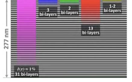
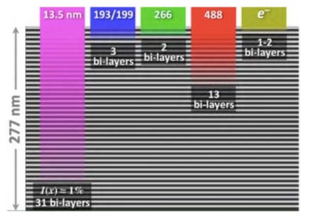
One of the most challenging points of inspecting EUV photomasks compared to DUV photomasks is detecting phase shift defects. The so-called “phase shift defects” are defects hidden between the multiple reflective layers of EUV photomasks (DUV photomasks do not have such multilayer structure). These defects disrupt the pitch of the reflective layer patterns and cause a phase shift in the light when EUV light is reflected. Only EUV light can detect phase shift defects that are deeply embedded in the multi-layer structure of EUV photomask, and other inspection wavelengths are only capable to detect defects in the top few layers (see picture below, the most left side shows the EUV wavelength of 13.5nm):
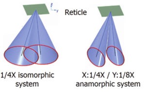
In addition, the future High NA EUV lithography will require new technological advancements in photomask inspection. There are two main differences between High NA EUV and Low NA EUV inspection: 1) Smaller Defects: High NA EUV defects are smaller, so the sensitivity (signal-to-noise ratio) of inspection tool must be improved meaningfully; 2) Optical System Changes: The optical system of High NA EUV is different. Specifically, achieving a higher numerical aperture means using larger mirrors. However, larger mirrors cause the incident angle of EUV light hitting the photomask to increase, and a larger incident angle significantly reduces the reflectivity of the photomask(eg. imagine the difference in reflectivity when a ray of light hits a flat surface from a near-horizontal angle versus a 45-degree angle),so the pattern can hardly be transferred to the wafer. This issue could have been addressed by shrinking the pattern by 8x rather than the 4x used in the current Low NA EUV system, but that would have required the use of a larger photomask, which would necessitate redesigning in the entire photomask-related ecosystem. To avoid the complexity of redesigning issue, ASML chose to keep the photomask size the same and instead change its optical system: Rather than uniformly shrinking the pattern being printed, High NA EUV system’s mirrors shrink the pattern size by 4x along the X-axis but by 8x along the Y-axis. This anamorphic optical design forms an elliptical light cone, which not only reduces the incident angle at which EUV light hit the photomask and solves the reflection issue, but also avoids the problem of overlapping incident light cone and reflected light cone (see figure below):
Of course, this anamorphic optical design led to another issue: half-field exposure. With High NA EUV, the field size for a single exposure is only half of that in Low NA EUV (because the length of the Y-axis is halved). It therefore takes High NA EUV twice as many exposures to pattern a single wafer as compare to Low NA EUV, and twice as many exposures could have meant twice as long to print a wafer. To address this, ASML increased the speed of its stages(wafer stage speed is doubled, and reticle stage speed is quadrupled). This ensures that the wafer throughput of the entire High NA EUV system remains the same as Low NA EUV, even though the number of exposures per wafer has doubled.
Returning to Lasertec, let's introduce the company's flagship producs:
MAGICS series – DUV mask blank inspection tool
MATRICS series – DUV mask inspection tool
ABICS series – EUV mask blank inspection tool
ACTIS series – EUV mask inspection tool (for wafer fab use)
MIAS series – EUV mask inspection tool (for mask shop use)
According to my understanding, the current installed base of Lasertec's EUV mask inspection tools is roughly as follows: Intel has 14 units, TSMC has 9 units, and Samsung has 3 units. For the EUV mask blank inspection tools, the installed base is approximately 9 units.
In the following paragraphs, we will explore different types of EUV light sources, Lasertec’s future competition landscape (vs. KLA & Zeiss), and the company’s order outlook.


