


Co-Packaged Optics (CPO) – The Next Big Thing for Nvidia (NVDA US)?

In the previous article that I wrote back in July this year (The Bonder War – An update on ASMPT (522 HK),BESI (BESI NA), Shibaura (6590 JP), Tazmo (6266 JP) and other advanced packaging equipment players), I mentioned that NVIDIA's next-generation CPO product would use a hybrid bonding process. Recently, there has been increasing interest in NVIDIA's CPO adoption, so today I will talk about NVIDIA's next-generation CPO product.
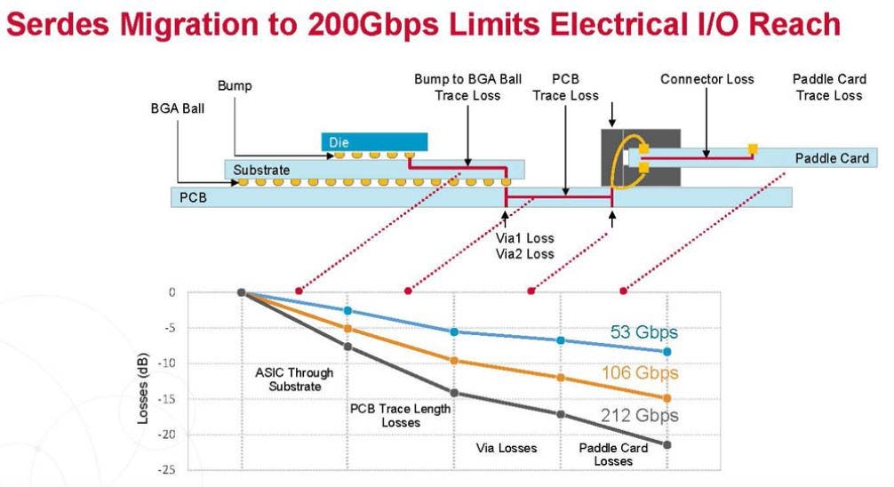
We know that as SerDes speed increases, the traditional solution of pluggable optical modules will have higher signal loss due to the use of multiple copper channels and longer distances to the chip (as shown in the figure below). Therefore, moving the placement of optical modules is the next-generation solution proposed by the industry. This involves integrating several optical modules into more compact optical engines and packaging them together with compute chips, which is the concept of Co-Packaged Optics (CPO).
Here, I want to first clarify a common misunderstanding by the market. NVIDIA’s first CPO product, set to be released next year, is not a CPO rack system (as shown below) that is highly anticipated by some people, but rather an Infiniband (IB) switch.
According to NVIDIA's latest product roadmap (see the switch section in the bottom row of the table below), the company plans to launch the Quantum 3400 X800 IB switch in Q4 2024. The traditional pluggable optical module version of this switch will begin mass production at the end of this year. In addition, what is not shown in the diagram below is that there is also a hidden CPO version of this IB switch planned, which will begin mass production in Q3 2025. This will be NVIDIA's first mass-produced CPO product. Development on this CPO version of Quantum 3400 X800 IB switch began in late last year, and it has already been demonstrated to customers, so its market launch is pretty certain. After the IB switch, NVIDIA also plans to launch a CPO version of the Spectrum 5 X800 Ethernet switch in 2026.

Now let’s take a closer look at the appearance of this CPO version of Quantum 3400 X800 IB switch: It is a 4U-height switch with six rows of 24 MPO (Multi-fiber Push On, a standardized optical fiber connector) ports per row. Each port supports 800G, so totalling 144 800G ports. Additionally, the switch has 18 external pluggable laser light source modules (ELS modules) on the lower left side of the panel, and the lower right side of the panel includes debug ports, serial ports, and LED indicators (see the first diagram below). It is designed as a fully liquid-cooled system, with the power supply located in the central rear of the back panel and cold water inlet and hot water outlet pipes on the sides (see the second diagram below, the blue section represents the cold water inlet, and the red section represents the hot water outlet).


Next, let me introduce the internal structure of this CPO version of Quantum 3400 X800 IB switch:
The Q3400 X800 CPO switch contains four 28.8T switch chips (with a total switching capacity of 115.2T). However, the four switch chips do not communicate directly with each other. Instead, they use multi-plane topology in the switch architecture. In multi-plane technology, each external optical fiber entering from the MPO port is split into four paths by fiber shuffle box and then connected to four different switch chips (i.e., four independent switching planes), which divides the data signal into the smallest unit. This architecture allows multiple independent switch planes to operate simultaneously (hence the name multi-plane) and the data is eventually aggregated at the CX8 network card end.
In other words, NVIDIA’s CX8 network card splits the data into four parts, each part is processed and forwarded by a different switch chip, without the need for an additional coordination mechanism, since each data sub-stream is handled independently and merged at the network card end. Compared to the single-chip architecture of traditional switches, this multi-plane architecture can effectively expand the number of ports a single-layer network device can support.
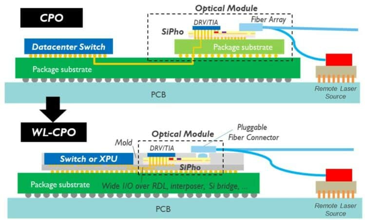
Inside the CPO switch, the CW laser in the ELS module transmits the signal directly to the fiber array through passive lens and thin-film filter, and then pulls it to the MPO ports on the switch panel (as shown in the diagram). This method functions as a relay between two fibers, directly transmitting the signal. In the upper half of the diagram, we can see the current solution used by NVIDIA’s CPO switch, where the switch chip and optical engine are packaged on the same substrate. In the next generation, NVIDIA will use the lower half of the diagram’s solution, placing the switch chip and optical engine on the same interposer to achieve wafer-level CPO (i.e. CoW).
The so-called optical engines can be regarded as integrated optical modules. By packaging optical modules into an optical engine, multiple traditional optical modules (such as four or eight) can be physically integrated into a single engine. These engines, packaged together with the switch chip on the same substrate (or in the future on the same interposer), transmit the optical-electrical converted signal directly to the vicinity of the switch chip. This reduces the required physical space and increases integration density of the switch. In my previous article (The Bonder War – An update on ASMPT (522 HK),BESI (BESI NA), Shibaura (6590 JP), Tazmo (6266 JP) and other advanced packaging equipment players), I showed a concept diagram of TSMC's optical engine:


Now we know that each switch chip inside NVIDIA’s Q3400 X800 CPO switch has a capacity of 28.8T, while each incoming optical fiber supports 800G (i.e., 0.8T). Hence, a single switch chip requires 28.8/0.8 = 36 channels. Each optical engine handles four channels (equivalent to handling four 800G optical modules), so each switch chip needs to be paired with 36/4 = 9 optical engines. Although pairing one switch chip with nine optical engines does not seem to match TSMC’s concept diagram above (which shows a 1:8 pairing), asymmetric layouts like this are not uncommon in practice. For example, some high-performance computing chip may have one side of the chip connecting to HBM (High Bandwidth Memory), while the other side connecting to optical I/O, leading to an asymmetric layout.
Last but not least, let’s take a look at the key suppliers list of this NVIDIA’s CPO switch:
Keep reading with a 7-day free trial
Subscribe to Global Technology Research to keep reading this post and get 7 days of free access to the full post archives.