

Preface:
About a year ago, when I started writing this newsletter, my initial goal was to introduce technological advancements or transformations in the tech industry to general readers in a way that was accessible and easy to understand, especially focusing on niche tech areas that mainstream media often overlook. My first few articles covered rather obscure topics, such as electronic fiberglass cloth and yarn(Nittobo (3110 JP) -- The King of Electronic Fiber Glass), temporary bonding and debonding(SUSS MicroTec (SMHN GR) -- A Hidden Advanced Packaging Play), plastic and glass lenses in optical modules(Enplas (6961 JP) -- Another Japan Fake AI Play?), among others. However, readership during the first six months was underwhelming.
After consulting friends, I realized that to attract readers, I had to write about popular and widely discussed topics. Thus, I made some transition in the second half of the year to cover trending subjects, writing about NVIDIA & ASIC chips and system designs, which led to a meaningful increase in readership.
While I was pleased with these results, I also started feeling a bit fatigued by constantly chasing popular topics. Therefore, at the beginning of this new year, I want to return to my original aspiration. For the first article of 2025, I dedicate it to a very niche topic in the semiconductor industry: CNT pellicles.
In my future writing, I will strive to find a good balance between topics that general readers are interested in and those that I am passionate about. I hope to continue improving this newsletter and that you will enjoy reading my content.
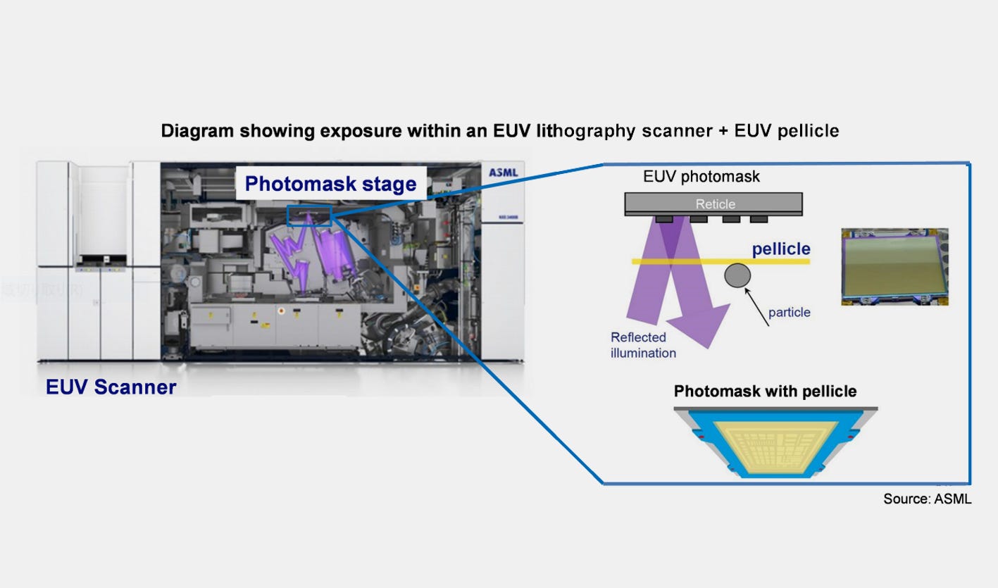
Now, let’s dive into the topic! In a detailed article last year, I explained the EUV mask inspection tool (Is Lasertec (6920 JP) a Short? – All you need to know about EUV mask inspection). Today’s article can be considered a sequel, where I will discuss another crucial yet lesser-known component in EUV systems: the EUV pellicle.
In typical semiconductor lithography process, a thin protective film is typically placed over the photomask surface to shield it from contaminants. This film, known as a pellicle, prevents undesirable occurrences or defects in wafer circuit patterns and thereby protects IC chips from potential damage (see the diagram below):
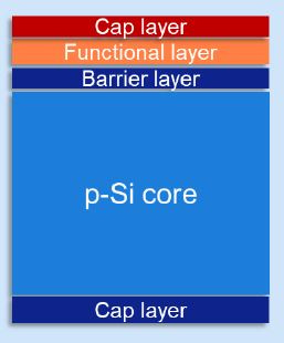
Initially, pellicles were single-layer structure with a core layer made from polysilicon. Above this core layer were two thin barrier and functional layers, and finally, a protective cap layer was applied on the top and bottom surfaces (see the diagram below):
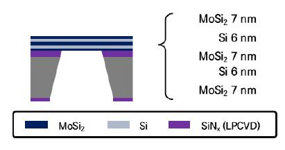
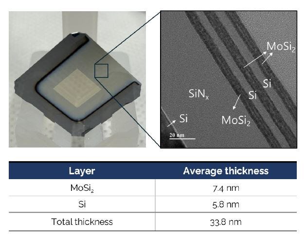
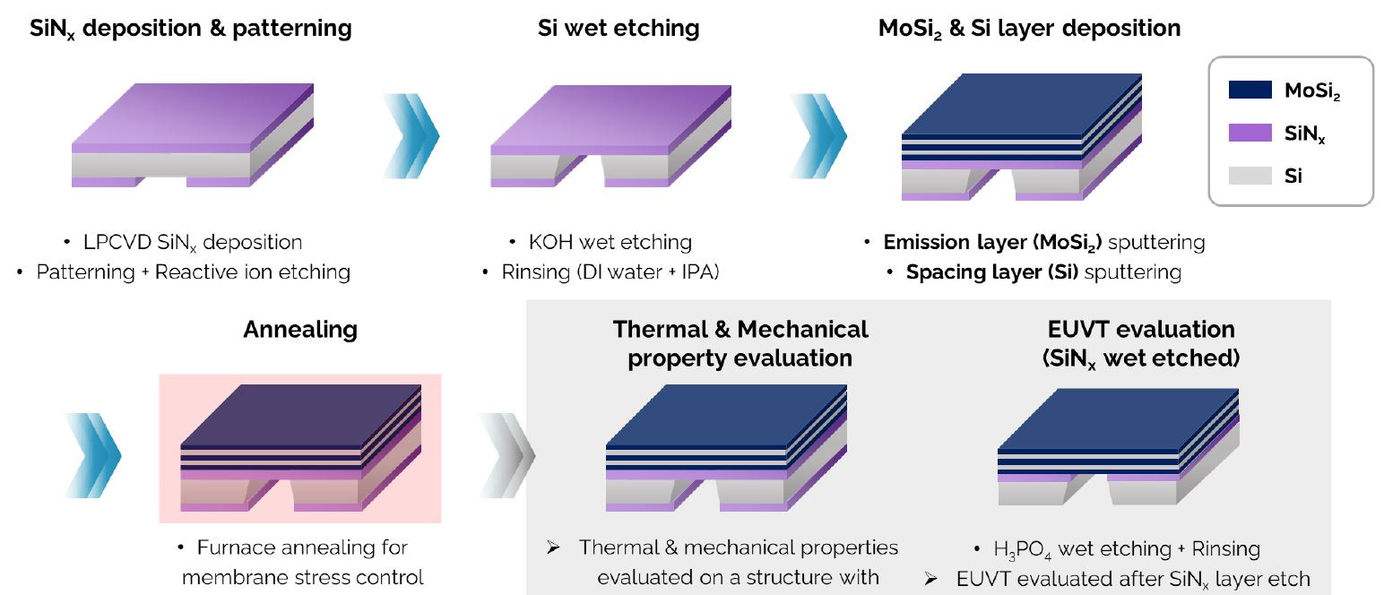
Since 2021, EUV pellicles have adopted composite materials. Its critical component now consists of alternating layers of molybdenum disilicide (MoSi₂) and silicon (Si), forming a multi-layer structure. The MoSi₂ layers (emission layers) have three layers, each 7.4nm thick, while the silicon layers (spacing layers) have two layers, each 5.8nm thick, with a total thickness of 33.8nm (see diagrams 1 and 2 below):
EUV transmittance (EUVT) is a critical performance indicator for EUV pellicles. The transition from single-layer to multi-layer structures increased the EUVT from approximately 82% to around 90%. The diagram below shows the manufacturing process for multi-layer EUV pellicles:
The next iteration of pellicle technology goes beyond structural changes (from single-layer to multi-layer) and introduces advancements in materials, leading to the emergence of CNT pellicles (see diagram below):
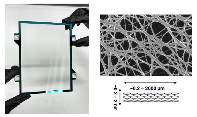
CNT pellicles, made from carbon nanotube materials, offer several advantages over traditional MoSi₂/ Si pellicles:
Higher power limit
Higher thermal stability
Higher EUVT
Let’s explore these advantages one by one.
1. Higher Power Limit
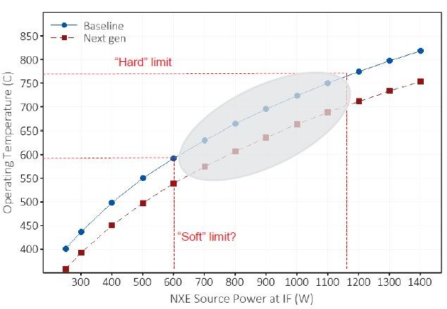
For EUV systems, higher power translates to higher throughput, and each generation of EUV machines aims to achieve greater power levels (see diagram below):

However, higher power can damage conventional pellicle materials. The industry generally defines the power limit of EUV pellicles into two categories:
Hard limit: The power level at which the pellicle will break.
Soft limit: The power level beyond which material degradation begins to affect pellicle uniformity, impacting chip exposure patterns.
The existing MoSi₂/ Si pellicles have a soft limit around 600W and a hard limit around 1100W (see diagram below). In contrast, CNT pellicles have power limit easily exceeding 1000W, aligning well with the roadmap for future high-power EUV systems:
2. Higher Thermal Stability
During CNT material production, metal catalysts are typically added to aid carbon nanotube materials growth. These catalyst particles decompose hydrocarbons, which then dissolve into the particle and form a liquid eutectic. When the eutectic becomes supersaturated, carbon precipitates out in a tubular, crystalline form. However, for EUV pellicles, metal catalysts are considered impurities. Thus, high-temperature pre-exposure vacuum annealing is necessary to purify the CNT film and remove contaminants and catalyst particles from CNT, enhancing the film’s transmittance and stability during EUV exposure (see diagram below):
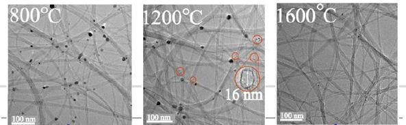
This characteristic of CNTs—becoming more stable at higher temperatures—makes them ideal for EUV chamber environment, where high-power EUV source inevitably generates higher temperatures. While conventional pellicle materials cannot withstand such condition for long time, the elevated temperature actually help increase stability of CNT pellicles.
3. Higher EUVT
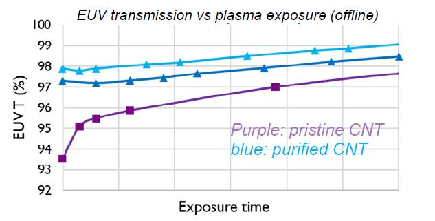
Traditional MoSi₂/ Si pellicles have an EUVT of ~90%. However, CNT pellicles pretreated with high-temperature vacuum annealing can achieve EUVT levels of 97–98% (see diagram below, the purple line is pristine CNT pellicle and the blue lines are purified CNT pellicles):
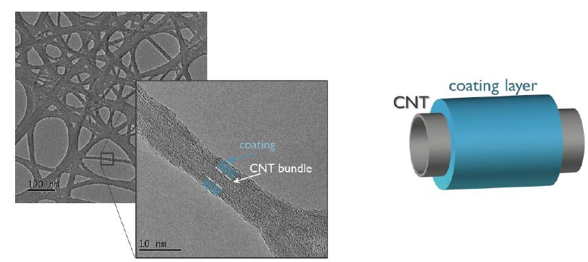
One challenge for CNT is that EUV generates highly reductive hydrogen plasma, which can etch CNTs. To mitigate this, a metal coating is applied to CNT films (see diagram below):
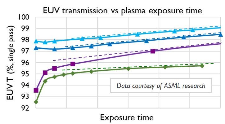
However, this metal coating reduces the EUVT of CNT pellicles to 95–96% (see diagram below, the newly added green line is the coated CNT pellicle). In practical exposure scenarios, where EUV light is reflected by photomask and passes through the pellicle twice, the effective EUVT is 95~96% x 95~96% = 90~92%.
Even so, CNT pellicles still outperform traditional pellicles, especially at higher power levels. As mentioned above, the existing MoSi2/ Silicon EUV pellicle cannot withstand high temperature environment for long time. Therefore, when EUV power reaches above 500W, the traditional EUV pellicle needs to be coated with a CDL layer for heat dissipation, but this CDL layer will also reduce EUV transmittance, so the actual EUVT of MoSi2/ Silicon pellicle used for EUV above 500W is only 90% x 90% - 7% = 74%, which is much lower than the 90~92% of CNT pellicle.
Some might question whether CNT pellicles will actually be widely adopted in the future, given the fact that the current EUV pellicle usage case is quite limited. Not only do memory manufacturers not use EUV pellicles, but even TSMC tries not to use EUV pellicles too much in their advanced node process, due to their high cost (over $10,000 per piece) and short lifespan (typically each need to be replaced every 3–4 days).
However, based on my supply chain research, TSMC plans to use CNT pellicles for its N2 process. If N2 mass production proves successful, CNT pellicles will be widely adopted in their A16 process. In the following paragraphs, I will explain why TSMC, previously hesitant to adopt EUV pellicles, is now actively embracing CNT pellicles, along with market size estimates and the qualification progress of each CNT pellicle manufacturers.
Keep reading with a 7-day free trial
Subscribe to Global Technology Research to keep reading this post and get 7 days of free access to the full post archives.