


ASM Pacific Technology (522 HK) vs. Kulicke & Soffa (KLIC US) – Who is the Fluxless TCB Winner?

In my previous article on bonders (The Bonder War – An update on ASMPT (522 HK),BESI (BESI NA), Shibaura (6590 JP), Tazmo (6266 JP) and other advanced packaging equipment players), I mentioned that NVIDIA’s next-generation Rubin series products will use the next-generation TCB equipment, namely fluxless TCB, for the CoWoS-L CoW process. Recently, many readers have been asking about this topic, hence today’s article will talk about fluxless TCB.
Before formally introducing fluxless TCB, let's briefly review the evolution of chip packaging technology. The most traditional packaging technology is called wire bonding, where the chip is placed face-up and connected to the pads on the substrate through fine gold wires (see picture below):

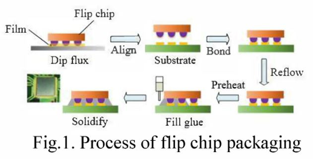
After that, the industry developed flip chip bonding technology in order to achieve higher I/O density. Compared to wire bonding, flip chip bonding involves flipping the chip upside down (hence the name "flip-chip"), and connecting it directly to the pads on the substrate through bumps. The key to this process is the bump-making processes, where reflow is an essential process. After bonding, the solder balls are not firmly placed on the packaging substrate until they are heated in a reflow oven, where the alloy material of the bumps melts and bonds tightly with the pads on the substrate. The temperature is then lowered to re-solidify the solder balls and complete the bonding (see picture below):
However, there is a troublesome issue in this reflow process: the different coefficients of thermal expansion (CTE) between materials. During the heating process of reflow oven, the materials expand at different rates, which may lead to some solder balls not fully contacting the copper pads, or the chip to be unevenly placed, or even leading to warpage of the substrate. These issues combined can ultimately result in decreased electrical performance or even failure of the packaged chip.
TCB (thermal compression bonding) is then invented to addresses these problems. Thermal compression bonders typically use individual tools to place the chip, apply pressure, and then heat the solder balls for bonding. The heat is applied only to the top of the chip, which minimizes the heat impact on the substrate and reduces the warpage issue. The pressure also ensures that the chip is placed flatly. (see picture below) Additionally, the rapid vibrations during the TCB process help to avoid particle contamination and voids in the underfill.

After wire bonding, flip chip bonding, and thermal compression bonding, we are now about to enter the fluxless TCB era. Kulicke & Soffa’s bonder product roadmap is a good example for this (see image below):
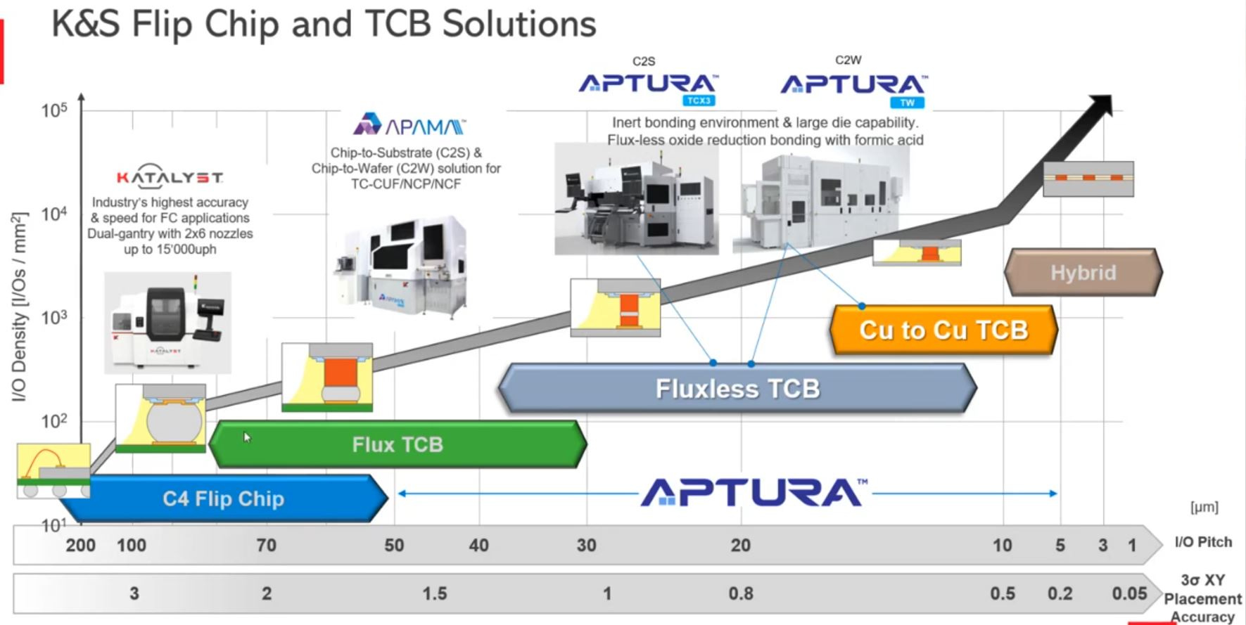
Traditional TCB process still uses flux underneath the solder balls (see image below), while fluxless TCB, as the name implies, eliminates the need for flux during thermal compression bonding. As shown in the technology roadmap above, the packaging I/O pitch has shrunk from 200μm to 30μm from flip chip bonding to flux TCB, and fluxless TCB will further reduce the pitch size to 20μm, with a maximum case of reaching 10μm. When the I/O pitch is smaller than 10μm, hybrid bonding is then required (for more details on hybrid bonding, please refer to my previous article: BESI (BESI NA) -- Where is Hybrid Bonding Used?).

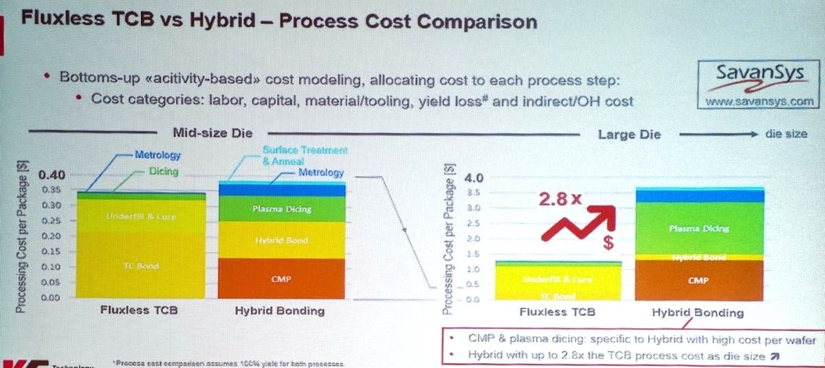
For I/O pitches between 10-30μm, fluxless TCB offers a meaningful cost-performance advantage compared to hybrid bonding. This is especially true for large die sizes, where hybrid bonding requires additional costly processes like CMP (HB has very high requirement of surface flatness, typically <0.5nm Ra) and plasma dicing (to prevent particle contamination during bonding, conventional blade dicing is prone to generate particles and hence cannot be used). These factors make hybrid bonding up to 2.8 times expensive as fluxless TCB in terms of cost per package (see diagram below):
Next, let's return to the main focus of this article and take a detailed look at the fluxless TCB process.
Traditional TCB uses relatively larger solder balls made of alloy, not copper, and hence requires flux. However, as bump pitches shrink to a certain point, the shape of the solder ball can no longer remain a complete sphere. Instead, it forms an arc on top of a copper pillar. In this case, the small amount of solder does not require flux (which is difficult to clean out), but there will be a thin layer of oxidation on the solder surface to protect it (see image below):

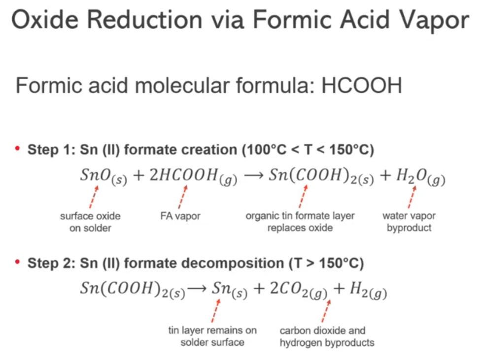
The fluxless TCB process begins with dividing the wafers into source wafers and TAC wafers, which are then transferred to a chamber. K&S uses a chemical method—formic acid—to remove the oxidation layer on the wafer’s surface, while ASMPT uses a physical method—plasma cleaning. After the oxidation layer is completely removed by plasma or formic acid, the exposed arc-shaped solder is ready for thermal compression bonding.
The chemical equations below show how formic acid (HCOOH) reacts with the tin oxide (SnO) on the solder surface under different temperature conditions, in order to remove the oxidation layer:
At the Semicon Taiwan exhibition held in September this year, K&S, as a keynote speaker on advanced packaging, presented the advantages and disadvantages of the two fluxless TCB technologies: formic acid vs. plasma (see table below). Of course, as a proponent of the formic acid technology, K&S’s presentation might be somewhat biased. Nevertheless, what I learnt from my supply chain research is roughly in line with the information below:

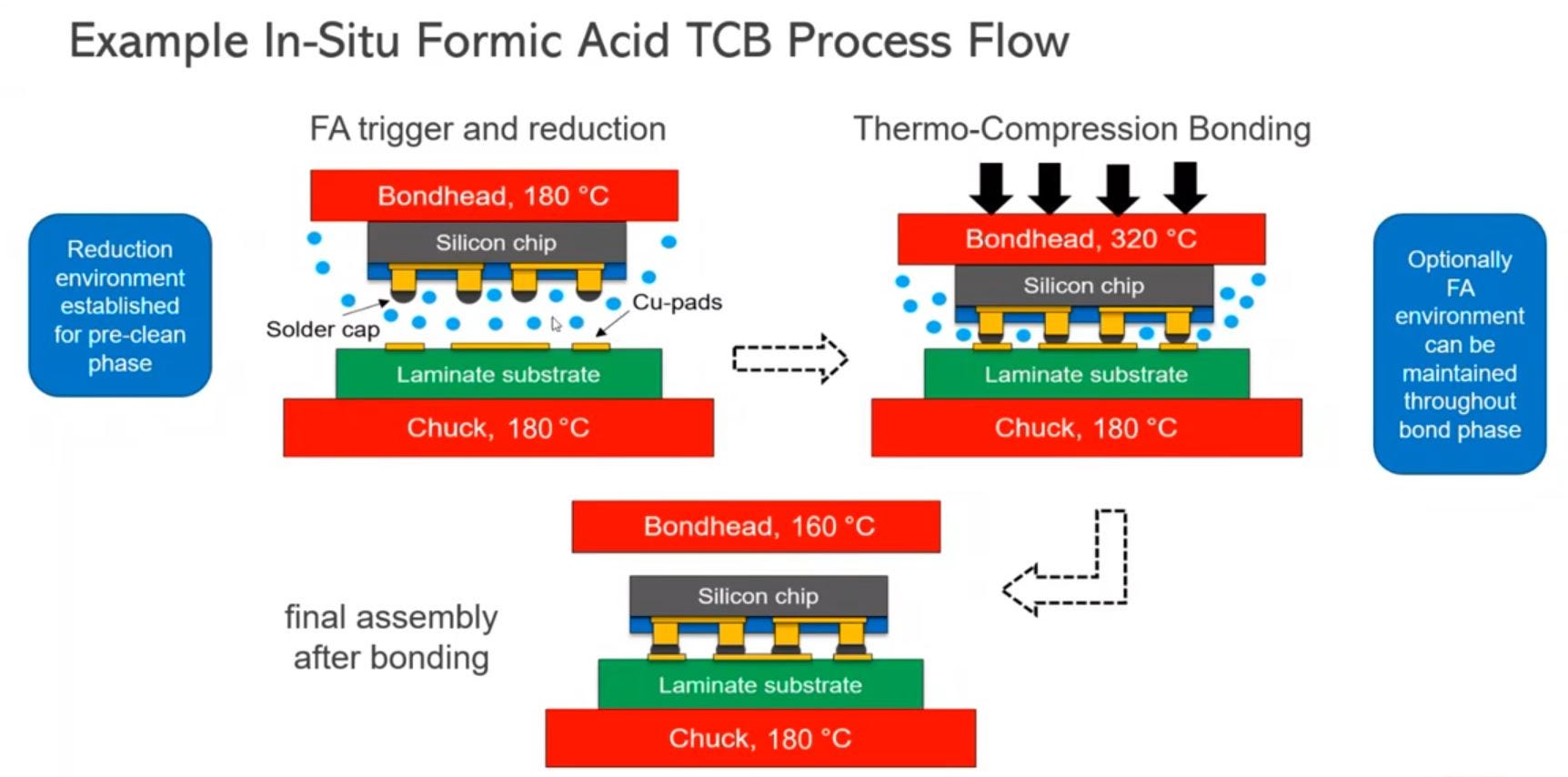
The advantage of K&S’s formic acid method is that it can remove the oxidation layer while simultaneously performing thermal compression bonding, hence preventing the risk of re-oxidation on the solder ball surface (see image below). The disadvantage of the method is that the chemical process leaves behind residuals (as shown in the chemical reaction formula above), requiring an additional cleaning station after bonding to ensure yield (the smaller the bump pitch, the harder it is to clean the residuals thoroughly). This results in slower throughput of the tool.
ASMPT’s plasma method, on the other hand, offers higher throughput and does not require an extra cleaning station. However, the removal of the oxidation layer and thermal compression bonding cannot occur simultaneously. In this method, physical ions bombard the surface of solder balls to remove the oxidation layer first, and then thermal compression bonding is performed, leaving a risk of re-oxidation in between the two steps. Additionally, different plasma recipes need to be adjusted for different dies, making the process more complicated.
After analyzing the pros and cons of formic acid vs. plasma method of fluxless TCB, let's reveal which fluxless TCB equipment will eventually be used in NVIDIA’s next-generation Rubin series products:
Keep reading with a 7-day free trial
Subscribe to Global Technology Research to keep reading this post and get 7 days of free access to the full post archives.